Voltlog #201 – How To Generate Gerber Files and Order Your PCBs

Welcome to a new Voltlog, today I’m gonna show you how to order your pcbs from start to finish. We’re gonna start with generating the gerber files and walk you through the process up to placing your order on a pcb manufacturing service website.But before we get started I’ll take a moment to remind you that I now have a Patreon account so you can support me through Patreon to continue making more videos like this one.

The actual start might depend on the cad software that you use for designing pcb’s, in my case that’s Eagle Cad. After finishing up the design of a PCB, you will have to generate the gerber files needed to place your order. Think at these as an universal set of files, stored in a format that every pcb manufacturing facility can read and use to manufacture your pcb exactly as you designed it.

In Eagle CAD we have the CAM processor that takes care of these things, and luckily you can just load a pre-made CAM job file, that will instruct eagle how to output a complete set of gerber files. I have a custom made, voltlog CAM job file for 2 layer pcbs, I will place a link to it in the description below so you can download it. This cam job file will generate all the required gerber files for ordering your pcb, including files for the cream layer which can be used to order a steel stencil that will make assembly of surface mount components much easier.

Voltlog #161 – How To Assemble SMD Parts

In this video I’m gonna show you 3 methods to solder SMD parts but before we get to the actual methods I think it’s best to talk about the type of solder to be used. And there are two main types of solder that you can use, that is leaded or lead free solder. If you are doing prototype work it’s best to stick with leaded solder or solder paste because it’s easier to get right, it has a lower melting temperature. If you are doing production work, you plan to sell those boards, than you might be forced to use lead free solder to be compliant with the regulation.

Here are links to the items shown in this video:

EasyEDA PCB Service Review

I’ve talked about EasyEDA in the past in Voltog #58 where I reviewed their free online pcb design software. Now the guys from EasyEDA asked me if I wanted to review their pcb service and I said yes. They offered to fabricate my pcb’s for free and also included a steel stencil.

The design for these pcb’s is my dark load project, the electronic dummy load that I’ve started working on over a year ago but never got around to finishing the project. The main reason for not finishing the project was because I don’t like writing code that much so after spending some time on the STM32, writing code for testing the on-board hardware, initializing the OLED display and the ADC I got bored and kinda stopped working on the project.

However there were some hardware improvements that I planned to do on that design, especially with the fan pwm control circuit. I wanted to switch to an inverted buck dc-dc converter topology driven from the microcontroller with PWM. This way I would get a nice varying dc voltage that would reliably vary the speed to any type of dc fan connected, but that’s another story.

Just so it happens, I recently reviewed the pcb assembly service from 7pcb.com so I have a spare blank pcb from their service so we can use this pcb which is an identical design for comparison. The only difference is that EasyEDA does not offer a matte black soldermask finish so I had to go with normal glossy black on their service.

How is the ordering process on EasyEDA?

The ordering process is an important part that might help you decide whether or not you will order from a specific shop. If you go to EasyEDA PCB ordering page, you will be greeted with a simple layout, you just need to drag&drop your gerber files and select the various options for the pcb panel.

They let you select the quantity, pcb thickness, soldermask color, surface finish, copper weight, temp rating, holes/traces/spacing, pretty much standard options with every board house these days.

You can also check an option to get a steel stencil if you need it and in the end you will get a build time estimate, a price estimate and you can also simulate the shipping cost. In my opinion this is a pretty straightforward, easy to use ordering form.

I ordered two pcb designs: first was 100x60mm ($75 for 5pcs with steel stencil) second was 106x55mm ($57 for 5pcs), black soldermask, ENIG finish. The total cost was $132 plus shipping. Shipping to Romania via DHL was another $37.

How is the silkscreen quality?

Unfortunately I no longer have my microscope so I am only using a macro lens to take close-up pictures of the pcbs but we can still observe the silkscreen quality and resolution in the picture below.
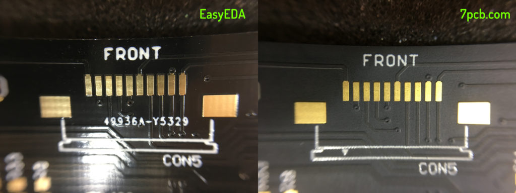
The vertical copper pads are 0.6×1.9mm in size and the text block saying “FRONT” is about 5.7×1.2mm. The printing on the 7pcb.com panel looks to be a bit sharper, not by much, just a bit. We can also notice EasyEDA placed some text under that connector on the top side of my pcb. Personally I don’t like it when they place text on my pcbs, but at least in this case they placed it under a connector where it would never get seen after the assembly.

Soldermask expansion and alignment

The soldermask alignment is not perfect but certainly acceptable and comparable between the two. It’s shifted on the same axis on both panels, but it doesn’t obstruct the copper pad in any way so that is perfectly acceptable, especially considering those passives are 0603 so the actual size is quite small.

The panel from 7pcb.com seems to have tighter tolerance for mask expansion and alignment but as I mentioned, the one from EasyEDA will work just as well as there is no pad obstruction happening.

No soldermask between the microcontroller pads for the EasyEDA panel while we have the mask on the 7pcb.com panel. I am not sure if 7pcb.com have a better more precise process for the soldermask application or is it just something specific to the matte black soldermask, maybe a different process specific to the matte black? Overall the soldermask print was uniform and without any scratches or problems on both panels.

Holes offset

This is where a microscope would of been handy because just with a macro lens is not really possible to get a feel for the holes offset.

These are 0.7mm drill holes in the fan connector and they look very well aligned on both panels. Maybe just a very small offset on the 7pcb.com panel but that is perfectly acceptable and won’t cause any trouble.

Overall very good drill hole alignment with no or very minimal offset on these two panels.

What about the steel stencil?

As mentioned in the start of this article I also got a steel stencil with this order to make the assembly work easier. There isn’t much you can review or say about a steel stencil. It was shipped nicely sandwiched between two pieces of plywood so it wouldn’t get damaged during shipping. It’s your standard frameless laser cut stencil that you can get from most pcb fab houses.
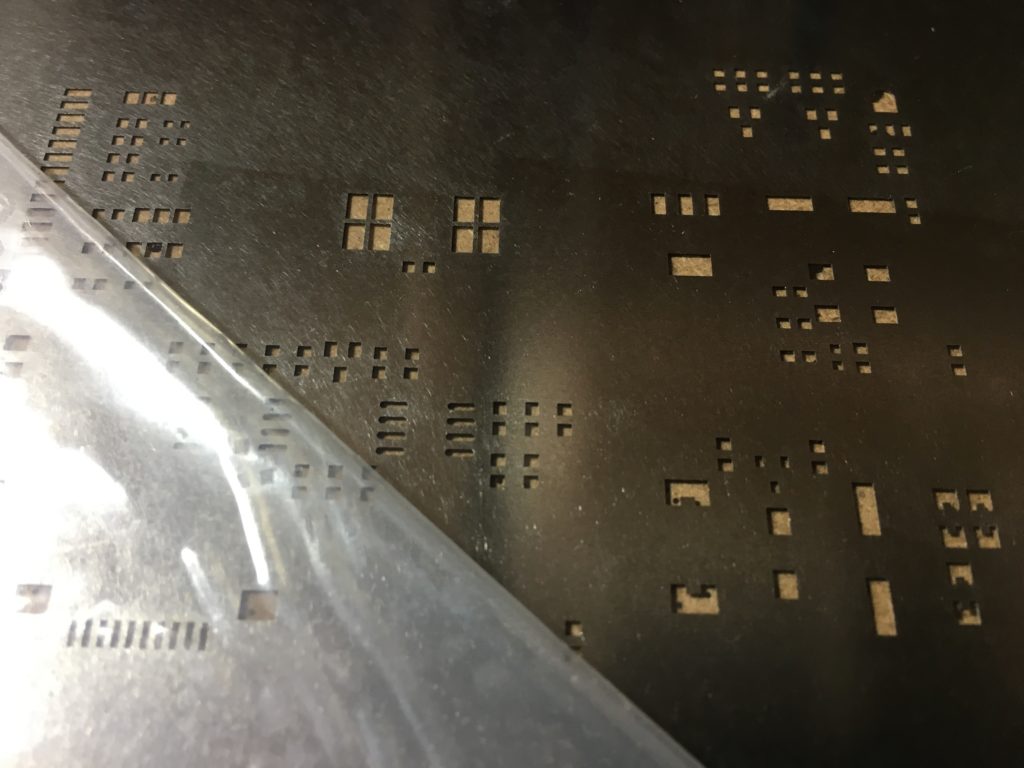
The specs for this laser cut steel stencil are: no frame, 0.12mm thick, no fiducials, no eletropolishing (electropolishing removes the micro burrs associated with laser cuts, leaving behind smooth aperture walls for easy transition of paste from the stencil to the pads), 280×380 size for a cost of $17.9 and 0.7Kg added to the shipping weight. On their website you can select multiple options but I went with the standard ones.

Conclusion

Although I don’t have any cost information on the 7pcb.com panel, I think the price should be similar so it was a fair comparison.  In terms of the ordering process EasyEDA have clearly invested in their online platform so the ordering process is very smooth and fast.

The quality of these pcb’s is very similar but the one from 7pcb.com stands out in a few areas like silkscreen quality and soldermask expansion and alignment.

Should you order pcbs from EasyEDA? I’m tempted to say the pcb’s from EasyEDA would directly compete with the ones offered at a lower price by shops like SeeedStudio Fusion, Elecrow, DirtyPCBs, and others. A fair comparison would be to order the same pcb from one of these lower cost shops and check if they are the same quality. If they are the same quality then, I wouldn’t recommend buying something more expensive unless you benefit from something else like the ordering experience.

For example if you are using EasyEDA online cad tool, then it would simply be a matter of a few clicks to get your design into production. In that case it might be worth to pay extra because it will save you time.

I think hobbyists who usually don’t need any extra bells and whistles will continue to order from the cheapest service available because they just need one-off pcb designs for their small projects and they don’t care how fast the order is processed or how the ordering process goes, they just want the cheapest option possible.

PCB Assembly Service Review 7pcb.com

I wrote this article to review the pcb assembly service offered by 7pcb.com (Bittele). They offered me a free of charge, complete turn-key pcb assembly service. I will start by discussing the advantages and disadvantages of professional pcb assembly services and then I will review the quality of the actual pcb they assembled for me. So if you are only interested in the review you can skip the first part.

Advantages of professional pcb assembly

If you are thinking about doing the pcb assembly in-house at a professional level you are quickly going to realize the initial investment cost is very high. You will need a minimum of: one pick and place machine, one stencil printing machine and one reflow oven. You probably also want other related equipment for inspection work and hand soldering tools. You will also need manpower and expertise which could raise the investment cost considerably. And finally when you consider there is very little ROI from this kind of investment you will quickly decide to outsource the pcb assembly service. In most cases outsourcing the pcb assembly service to an external company should be more cost effective.

Then there is the aspect of quality; a company specialized on pcb assembly services will have the expertise and manpower to provide excellent quality. They will also invest in their development by always having the latest technology so you the customer get all the benefits from the new assembly technologies. It is likely that you will hit a equipment related limitation doing in-house assembly if you do not upgrade the equipment regularly, for example you might end-up in a situation where you cannot reliably assembly the latest BGA package for a new processor.

There is also the aspect of quality control. A reputable pcb assembly house will also have a good established quality control service which you might benefit from by not having to do the quality control in-house. Sure you might want to do an extra quality control step in-house but it’s good to know at least the pcb’s are all functioning correctly when they leave the assembly line.

Disadvantages of professional pcb assembly

  • One reason you wouldn’t want to outsource the assembly of your project is to protect intellectual property. If you are working on some top secret project or the newest idea that will revolutionize something, you might want to keep that as secret as possible so in that case you might do the pcb assembly in house.
  • There are also cases when the turnaround time of a prototype is critical so you might not afford to wait a week for your pcb to come back from a professional assembly line. In that case it might make more sense to do the assembly in house.
  • Cost is also an important reason you might not want to go with a professional pcb assembly house, especially for small businesses or hobbyists. Prices for pcb assembly services have lowered considerably in the past few years so this is less of an issue these days but still you won’t see too much individuals sending their one off hobby projects to a board assembly house.

How is the ordering process?

When working with board assembly houses they will generally start by requesting 3 things from you: the gerber files for fabricating the pcb(including the solder paste layer for creating a stencil), the component placement list and a BOM(bill of material), The pcb I used for this review was designed in eagle so I had to export the gerber files using the cam processor, next I generated the component placement list using mountsmd.ulp. I continued with generating the BOM by running bom.ulp.

I sent these files by email to someone at 7pcb.com and part of their process is to run an initial DFM (design for manufacturing) check. They detected I had in my bom an inductor that was larger in size than the actual placement I used on the PCB. Luckily they notified me about the issue and I was able to correct that but due to my mistake another day was added to the total processing time.

Another thing to consider when outsourcing work to China is their local holidays. It happened that this collaboration started right before the Chinese new year holiday. So if you are in a hurry don’t order something just before their holidays because that will add delays to the processing time. If I were to exclude the holiday, I think from start to finish they took about 10 days to assemble this board, and that includes the full service: pcb manufacturing, parts sourcing, my mistake with the inductor and the actual assembly.

Review

My design of the pcb originally included a mix of 0805 and 0603 passives but since was going to be assembled in a pick and place machine that can handle the smallest passives easily I designed to switch everything down to 0603. This way it’s small enough to easily place passives close to other components and it’s still accessible for debug & probing.

On the pcb I had a mix of smd and through hole parts and that is not desirable if you want to lower the cost. Generally speaking placing smd components is cheaper than soldering through hole parts. In my case, since this was a review, it didn’t matter because they offered me a free of charge service but you might want to optimize your design for manufacturing and include only smd components.

BOM consolidation is another aspects that might lower your cost. Instead of using separate 10K, 11K and 12K resistor, see if you can use 10K for all of those resistors. Same goes for all the passives on your board, try to use as few different values as possible because the final cost will depend on the number of different values you use.

The assembled board was packed very nice with lots of foam protection and inside an antistatic bag. Shipping was done by FedEx so it arrived very quickly.

I wanted a matte black soldermask finish and I know there are not allot of pcb houses that offer a matte black finish but it seems they work with one that does. As you can see in the picture above it looks very nice with this finish.

Component placement and alignment seems to be perfect and that is to be expected from a good quality pick and place process. I asked 7pcb.com and they said every pcb goes through the pick and place machine even if it’s a single piece that gets assembled.

The through hole components were hand soldered, that is the usual process with small volume runs. But look at the solder joints, they look perfect. The person doing this is certainly very experienced and was probably using very good tools and materials.

Regarding the solder paste and the solder wire used in the assembly, they are no-clean, low residue, lead free. The no-clean part is important, as you can see from the previous 4 images, there is very little flux residue left from the soldering process so the board doesn’t need to go through an extra cleaning step. The lead free part is important for meeting current regulations regarding the usage of hazardous substances in electronics.

Even the fine pitch components like this 64 pin LQFP microcontroller is perfectly aligned and soldered. It seems like they have a pretty good process because these joints look like top quality.

The big bluetooth module that you see missing on the board was left out because I am using one of those cheap HC-05 bluetooth modules from ebay. This kind of module cannot be sourced from a known supplier, only from ebay and grey market china and 7pcb.com do not source parts from those sources. It was either send them the part or leave it out. Sending them the part would have taken too long so I decided to leave it out and just assemble it after I receive the board.

I was curious what was the cost for assembling this board, what would it cost me to have this board assembled if I were to pay for it? They said the cost is $336, this includes all NRE and setup charges. This will reduce significantly as you order more pieces because a big part of the cost are those setup charges. To this cost you would add the BOM cost, which in my case was something like $25 on DigiKey.

Voltlog #58 – EasyEDA Free Online PCB Design Software Review

The guys from EasyEDA contacted me and asked if I could do this review I accepted and they’re also going to be offering some free coupon codes for my viewers which you can use to order PCBs but more on that towards the end of this video.

EasyEDA being a cloud app it’s supported on every platform / operating system. You get schematic capture, circuit simulation and pcb layout functionalities. You can import files or projects created with other design tools like Eagle, Kicad or Altium and i’m sure it does most of the things that every pcb design tools does.

You can share and collaborate with other people on your projects so that’s a big selling point for EasyEDA and they made sure to put that on their front page. And I’m sure a bunch of other features that are not mentioned on their homepage and best of all you always get to work with the latest version because the app is on the server not on your computer. Another good thing is that you have the whole process from design to finished PCB on one single app or service and you just click through until you get the PCBs at your door and that might be a big advantage for some people.

Now, ofcourse a big concern with these kind of web based apps is what happens if they decide to shutdown the service? Well the guys from EasyEDA say that if they ever decide to shutdown the service they will open source the code and allow people to download all their projects so in theory you are covered, you could host your own server if that ever happens.

For more info, you should watch the video below.

Voltlog #36 – The Dark Load PCB Layout With EagleCAD

This video is mostly a time-lapse of me doing the PCB layout for the Dark Load project that I am working on. However during the first minutes of the video I am commenting and giving some hints on some design decisions that I make during layout.

This entire design is open source and it will be shared once I have it working but for now it’s still quite beta and I don’t want to release something that is potentially not working or might contain errors.

Review PCBcart vs OSH Park vs Smart Prototyping

This review/comparison might seem unfair at first because the PCB’s I got from PCBcart do not exactly count as hobby pcb’s due to their features and higher value but some of you might not put cost first on their list we can still get some useful points out of comparing these three.

I was working on designing a pcb for a new project when I was approached by someone at PCBcart who asked if I was willing to review their pcb service. I said yes and they offered to manufacture and send me the pcb’s for my project for free.

The price calculator and ordering system is fully automated on their website, you just fill in the details, you get a price quotation, next you upload your gerber files and place your order. A day later after submitting my files I was contacted by someone who was reviewing my gerber files. They noticed I had routed slots in the milling layer so they asked if they should route those through the middle of the marking line or in another way, thus getting the intended finished slot dimension.

They also noticed I had some square smd test points/pads which were also present in the stencil/paste layer and they asked if I want those in my stencil or not. This is something you might overlook and you might not want those present in your stencil if you plan on using those pads for programming, for example with some pogo pins in a jig. If that’s the case you want your pogo pins to touch directly the pcb pad, you don’t want any solder in between.

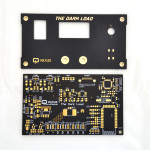
After exchanging some emails on those points my order went through manufacturing and I was notified it has been shipped with DHL. About 5 days later I had the boards in my hands and let me tell you these must be the most beautiful PCBs I ever had manufactured.

the dark load pcbcartthe dark load pcbcart the dark load pcbcart


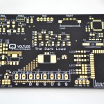
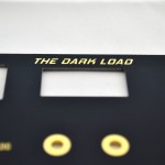
This is mostly due to the nice gold plating and the matte black soldermask. Definitely perfect for making front panels as I intended for one of these pcbs.

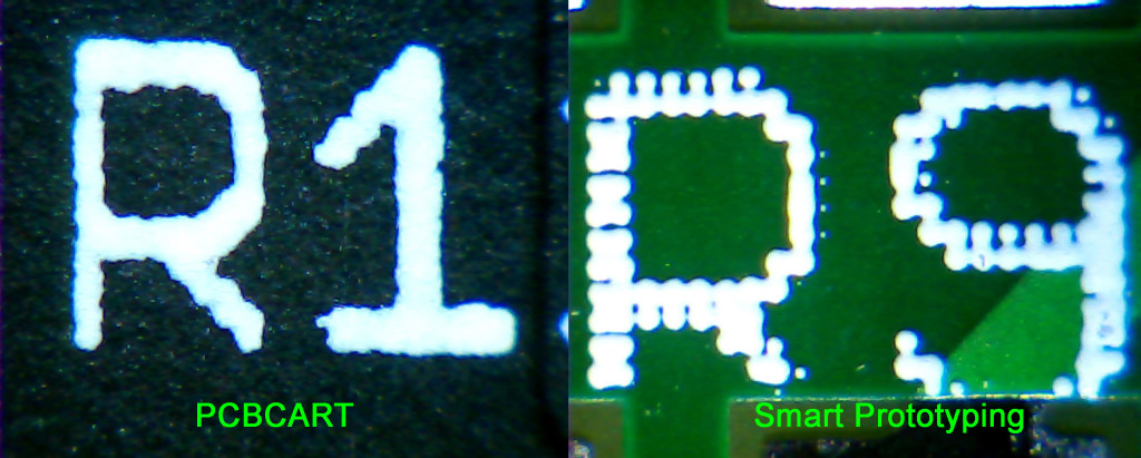
So let’s go through some things and compare these 3 pcbs. First let’s take a look at the quality of the silkscreen. All three have white silkscreen and I tried to get similar sized text for comparison. All images have been captured under my low cost microscope, at the same magnification level on the same flat bed surface.

Unfortunately the pcb from OSH Park doesn’t have any silkscreen, I don’t remember why, it was a prototype I did a while ago. The most likely scenario is that I forgot to export the silkscreen layer in my gerber files.

silkscreen-pcb-comparison

In this case, the result is quite clear, much better printing from PCBCART, they seem to have a higher resolution print. Most of you might not care to pay extra just for a better silkscreen but then again there might be some people who are designing for example a front panel pcb which needs a nice higher resolution silkscreen.

Next let’s take a look at soldermask alignment. In this category we can compare all three, and let me explain first that, with bigger mask relief (that is the clearance from mask to exposed copper pad) it is easier to handle offsets of the soldermask with regard to the actual copper layer. So I think, manufacturers that can’t maintain a tight tolerance on their mask alignment just increase the relief to make sure the mask never accidentally covers what should be an exposed pad.

soldermask tolerance

On this point, PCBCART again seems to be the best, I don’t even know what kind of process they use, but judging from the photos that I could get with my microscope, it looks like the soldermask extends right up to the copper pad with perfect alignment.

The spacing between the copper pads is also marked on the image and that is something to consider because with very low spacing some manufacturers cannot guarantee soldermask in between those pads. Having no soldermask in between pads might affect your soldering quality, you might get solder bridges more often for example. And in this test, the pcb from Smart Prototyping doesn’t get any soldermask in between those pads.

Next, let’s take a look at via/hole registration. This becomes quite important when working with small drill sizes like 0.3mm and below. You want your pcb to have that hole drilled right in the middle of the pad/via to ensure even copper distribution around it.

pcb-via-hole-registration

Starting from the left, we have PCBCART with a 0.5mm drill via, with excellent registration, clearly the winner judging by the even copper surface all around the drill hole. Next we have OSH PARK with 0.3mm tinted via, very good registration, no problem at all. And on the right we have Smart Prototyping probably 0.4mm drill tinted via, with a small offset.

And just for fun let’s take a look at one more thing, routed slots. In both PCBCART and Smart Prototyping boards I have some routed slots and the idea to compare this came to mind while holding the boards in my hands, I noticed one of them had cleaner slots, with less rough edges. I tried capturing this under the microscope but the results are not that great.

pcb-routed-slots-finish

The one from Smart Prototyping seems to have some rough edges on the inside of the routed slots but once again this is just something i noticed while playing with these pcbs, probably not something you would be worried when ordering your next pcbs.

So to conclude my experience with PCBCART, their website is great, you get all the info you need there and the process of ordering is very streamlined. Their customer support was very professional, not wasting time at all and the pcb quality was superb, the pictures speak for themselves.

And one other thing I liked about them, you know those nasty identification numbers that every pcb manufacturer puts on your pcb so they can identify it through their manufacturing process? Well sometimes we are designing front panels, and we don’t want those numbers visible on our pcbs and so far, no manufacturer ever listened to my request, not by email and not by a readme file archived together with the gerbers files. They all went ahead and put those numbers on my pcbs regardless of my request.

Well, pcbcart was the first ever to actually follow my request and not place any additional markings on my pcbs.

And if you’re curious about what the Dark Load is, subscribe to my voltlog youtube channel as more information will be posted there in an upcoming video.