This review/comparison might seem unfair at first because the PCB’s I got from PCBcart do not exactly count as hobby pcb’s due to their features and higher value but some of you might not put cost first on their list we can still get some useful points out of comparing these three.
I was working on designing a pcb for a new project when I was approached by someone at PCBcart who asked if I was willing to review their pcb service. I said yes and they offered to manufacture and send me the pcb’s for my project for free.
The price calculator and ordering system is fully automated on their website, you just fill in the details, you get a price quotation, next you upload your gerber files and place your order. A day later after submitting my files I was contacted by someone who was reviewing my gerber files. They noticed I had routed slots in the milling layer so they asked if they should route those through the middle of the marking line or in another way, thus getting the intended finished slot dimension.
They also noticed I had some square smd test points/pads which were also present in the stencil/paste layer and they asked if I want those in my stencil or not. This is something you might overlook and you might not want those present in your stencil if you plan on using those pads for programming, for example with some pogo pins in a jig. If that’s the case you want your pogo pins to touch directly the pcb pad, you don’t want any solder in between.
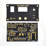
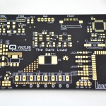
After exchanging some emails on those points my order went through manufacturing and I was notified it has been shipped with DHL. About 5 days later I had the boards in my hands and let me tell you these must be the most beautiful PCBs I ever had manufactured.


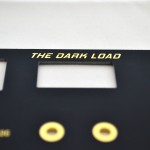
This is mostly due to the nice gold plating and the matte black soldermask. Definitely perfect for making front panels as I intended for one of these pcbs.
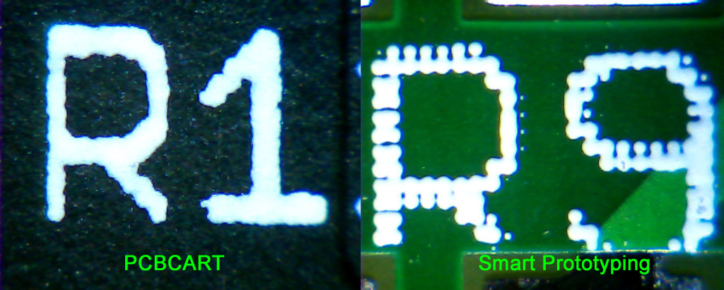
So let’s go through some things and compare these 3 pcbs. First let’s take a look at the quality of the silkscreen. All three have white silkscreen and I tried to get similar sized text for comparison. All images have been captured under my low cost microscope, at the same magnification level on the same flat bed surface.
Unfortunately the pcb from OSH Park doesn’t have any silkscreen, I don’t remember why, it was a prototype I did a while ago. The most likely scenario is that I forgot to export the silkscreen layer in my gerber files.

In this case, the result is quite clear, much better printing from PCBCART, they seem to have a higher resolution print. Most of you might not care to pay extra just for a better silkscreen but then again there might be some people who are designing for example a front panel pcb which needs a nice higher resolution silkscreen.
Next let’s take a look at soldermask alignment. In this category we can compare all three, and let me explain first that, with bigger mask relief (that is the clearance from mask to exposed copper pad) it is easier to handle offsets of the soldermask with regard to the actual copper layer. So I think, manufacturers that can’t maintain a tight tolerance on their mask alignment just increase the relief to make sure the mask never accidentally covers what should be an exposed pad.

On this point, PCBCART again seems to be the best, I don’t even know what kind of process they use, but judging from the photos that I could get with my microscope, it looks like the soldermask extends right up to the copper pad with perfect alignment.
The spacing between the copper pads is also marked on the image and that is something to consider because with very low spacing some manufacturers cannot guarantee soldermask in between those pads. Having no soldermask in between pads might affect your soldering quality, you might get solder bridges more often for example. And in this test, the pcb from Smart Prototyping doesn’t get any soldermask in between those pads.
Next, let’s take a look at via/hole registration. This becomes quite important when working with small drill sizes like 0.3mm and below. You want your pcb to have that hole drilled right in the middle of the pad/via to ensure even copper distribution around it.

Starting from the left, we have PCBCART with a 0.5mm drill via, with excellent registration, clearly the winner judging by the even copper surface all around the drill hole. Next we have OSH PARK with 0.3mm tinted via, very good registration, no problem at all. And on the right we have Smart Prototyping probably 0.4mm drill tinted via, with a small offset.
And just for fun let’s take a look at one more thing, routed slots. In both PCBCART and Smart Prototyping boards I have some routed slots and the idea to compare this came to mind while holding the boards in my hands, I noticed one of them had cleaner slots, with less rough edges. I tried capturing this under the microscope but the results are not that great.

The one from Smart Prototyping seems to have some rough edges on the inside of the routed slots but once again this is just something i noticed while playing with these pcbs, probably not something you would be worried when ordering your next pcbs.
So to conclude my experience with PCBCART, their website is great, you get all the info you need there and the process of ordering is very streamlined. Their customer support was very professional, not wasting time at all and the pcb quality was superb, the pictures speak for themselves.
And one other thing I liked about them, you know those nasty identification numbers that every pcb manufacturer puts on your pcb so they can identify it through their manufacturing process? Well sometimes we are designing front panels, and we don’t want those numbers visible on our pcbs and so far, no manufacturer ever listened to my request, not by email and not by a readme file archived together with the gerbers files. They all went ahead and put those numbers on my pcbs regardless of my request.
Well, pcbcart was the first ever to actually follow my request and not place any additional markings on my pcbs.
And if you’re curious about what the Dark Load is, subscribe to my voltlog youtube channel as more information will be posted there in an upcoming video.
