In this article I’m gonna review a set of PCBs I ordered from PCBway.com which I got for free for the purpose of this review. I have done several other PCB reviews in the past so if you would like to check those out, here are some links. (link, link)
In the article I’m only going to discuss the printed circuit boards themselves and the quality aspects of the boards. I will also be doing a short video on the subject where I will be discussing the ordering process and some aspects of their website.
So here is a picture with the boards I ordered, this is a simple breakout board I designed to interface to an epaper display.

It has all the bypass capacitors and additional circuitry needed to generate some voltages for the display. The SPI interface is broken out to header pins for easy connection to a controller board. The interface with the display is handled through a 24 pin, 0.5mm pitch flat flex connector.
How good is the soldermask?
So let’s go through some things that make-up a printed circuit board and analyze their quality. First let’s look at the soldermask, which in our case is green. This acts like a shield for the copper tracks, prevents oxidation and also helps during soldering if it’s present between adjacent pads.
The soldermask has opening for each connection pad and ideally you want the soldermask perfectly aligned so it doesn’t cover any area that you want clear. In the picture above (please excuse the low quality) we can see the soldermask aligns almost perfectly with the pad, no problems whatsoever.
How good is the silkscreen?
Next let’s talk about the silkscreen, which represents the legend of the PCB. In this case the silkscreen is white, which gives a good contrast over the green background created by the soldermask. The silkscreen contains valuable information like part numbers or values. In high density designs you want to be able to print small silkscreen and still be readable.
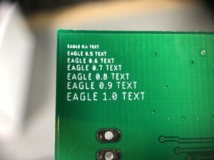
In the case of these boards I added different sized text on the back, and as you can see the text is clearly readable down to 0.5 text size in EagleCAD. I must say the quality of the silkscreen printing for these PCBs is excellent.
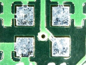
How are the drill holes aligned?
Another important aspect of a pcb are the drill holes and their alignment with corresponding pads. And here we need to take a look at the annular ring which is the circular area of a pad surrounding the drill hole. If you have a small via of just 0.2mm, the annular ring is very thin so it becomes very important for the drill to be exactly centered on the pad to avoid breaking the annular ring.
In the case of this design I specifically added a few rows of vias, starting from the left at 0.2mm, 0.3mm in the middle row and 0.4mm on the right row. This is so we can easily look at the quality and alignment of the drill holes.

In the close-up taken with my low quality microscope we can see the drill holes are well aligned with the center of the pad, on the 0.2mm vias and the 0.3mm ones, the holes are dead center with a perfect annular ring. We observer a slight deviation on the 0.4mm vias, which caused the annular ring to shrink on the left side of the pad but nothing to worry about, there is still plenty of copper in there.
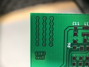
There are also a few less important things that we need to take a look at because I might consider them less important but they might be important to you. For example, identification labels. This is something all prototype pcb houses will add to your pcb. This is a code, they will add in the silkscreen and print on your pcb so they can later identify your pcb among others placed on a larger pcb panel. Sometimes they will add this code under a large part, so it will be invisible in the finished assembled board, sometimes, they just place it in plane sight.

In the image above you can see how PCBway added that text under the connector, so once I solder that flat flex connector, the identification text is not visible any more.
Electrical test?
And the last thing I would like to mention is the electrical test of the board. That is normally done with a flying test lead machine, which literally has flying test probes, moving really fast, checking each pad and track for connection or shorts. That action will leave small scratch marks on each pad and that is usually a good indication that the test has been performed. However in the case of prototyping services, the electrical test is usually nor performed because it takes time, it’s expensive and the pcb’s are cheap.
Normally these prototyping services just have an AOI step in their production flow. AOI stands for automated optical inspection and with the help of high resolution cameras it can identify most problems by comparing the resulted pcb with the original design file. I think these pcb’s we’re not subjected to electrical test but just AOI instead.
And to conclude my review of their pcb service I can say the PCBs turned out great, they are of good quality, nothing bad to talk about here. Regarding their website and ordering process, I think they can do a few things to improve the customer experience.
I also did a youtube video, talking about these PCBs, if you would like to watch that, I’ll include it below.


